The Industry Role of Backend Packaging Process


C.Y. LU | July 10, 2025
1. Introduction
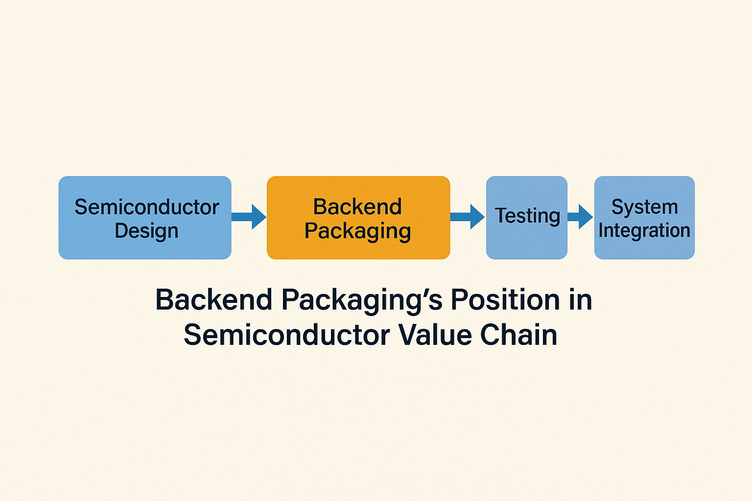
In the semiconductor industry, backend packaging has evolved from a passive post-processing step to a strategic enabler of system performance, miniaturization, and heterogeneous integration. As Moore's Law slows and integration complexity rises, backend packaging now plays a more critical role than ever in driving system-level innovation.
This document explores how packaging is shifting within the semiconductor value chain and examines its strategic implications across technology, manufacturing, and business models.
2. Problem Statement
Traditional packaging processes—such as wafer bumping, dicing, die attach, wire bonding, and molding—have long been considered labor-intensive and low-margin. However, the rise of advanced computing (AI, HPC), edge devices, and multi-die architectures (e.g., 2.5D/3D ICs, chiplets) is pushing packaging to deliver:
- Higher I/O density
- Better thermal performance
- Shorter signal paths
- Support for heterogeneous integration
Key challenges include:
- Integration of dies from multiple nodes and foundries
- Yield loss due to fine-pitch interconnects and ultra-thin dies
- High capital intensity of advanced packaging equipment
- Insufficient design and simulation capabilities among traditional OSATs
These gaps put traditional Outsourced Semiconductor Assembly and Test (OSAT) providers at risk of being bypassed by foundries and system companies offering in-house packaging.
3. Current State Assessment
Leading OSATs (e.g., ASE, Amkor, JCET) are transitioning to offer higher-value packaging solutions, including:
- Fan-Out Wafer-Level Packaging (FOWLP)
- 2.5D/3D integration with TSVs
- System-in-Package (SiP) modules
- Integrated thermal and EMI solutions
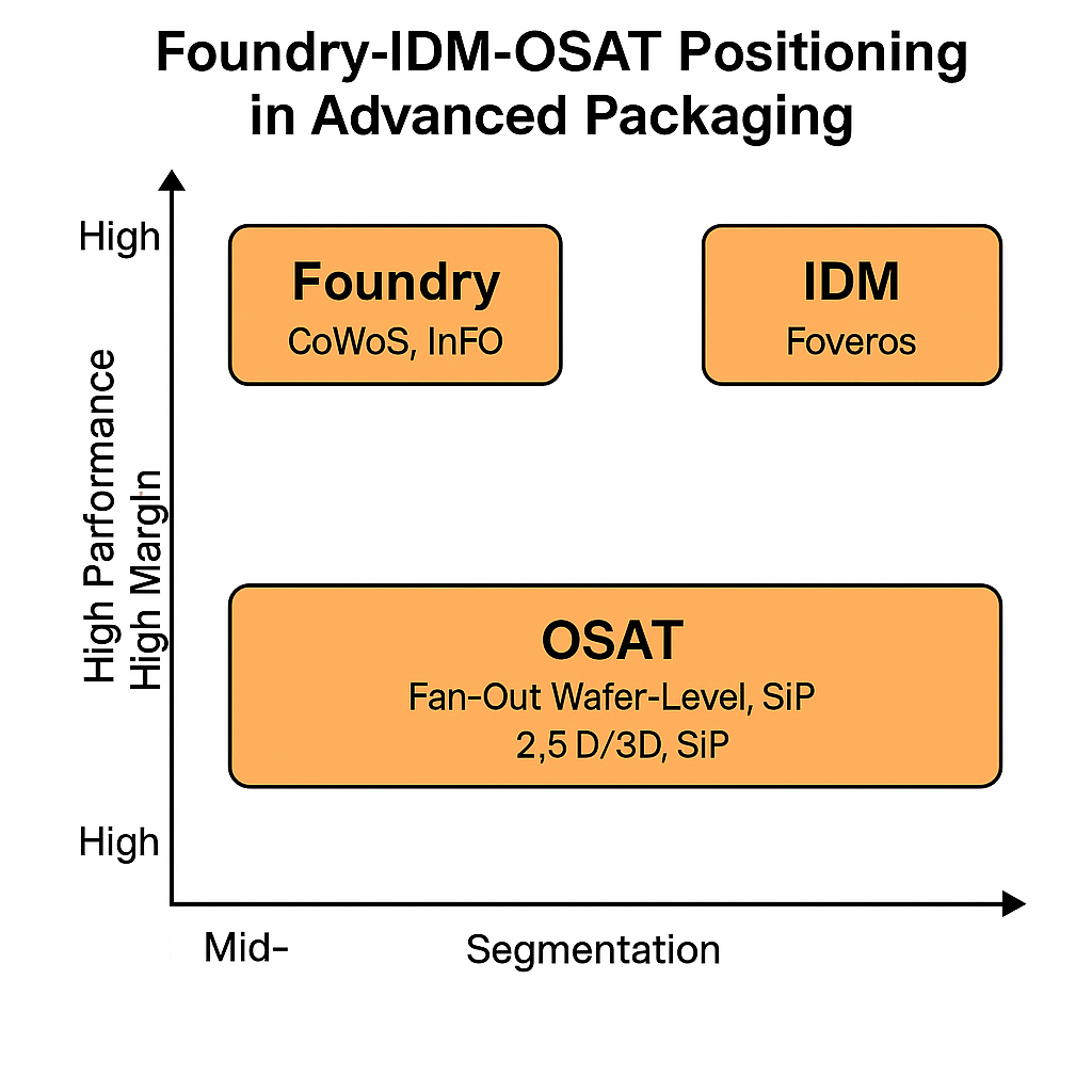
Meanwhile, foundries like TSMC (CoWoS, InFO) and IDMs like Intel (Foveros) are integrating packaging into their offerings, leading to a clear bifurcation:
- High-performance, high-margin packaging → Captured by foundries and IDMs
- High-volume, mid-range packaging → Remains with OSATs
Emerging markets (e.g., automotive, AR/VR, medical AIoT) offer growth potential but demand greater design collaboration, substrate innovation, and thermal reliability from packaging providers.
4. Proposed Solutions
To avoid marginalization and capitalize on next-generation system integration, backend packaging firms should pursue the following strategies:
- Develop heterogeneous integration platforms: Invest in FOCoS, chiplet assembly, and hybrid bonding.
- Strengthen design and simulation support: Build co-design platforms with system designers and foundries.
- Partner with materials and substrate innovators: Solve bottlenecks in high-density RDL, glass cores, and thermal interface materials.
- Integrate with ecosystem partners: Establish design hubs near fabless clusters (e.g., Hsinchu, Silicon Valley) for faster iteration.
This figure outlines the ecosystem of backend packaging, mapping key players, roles, and design collaboration workflows:
🔹 Key ecosystem players:
Category | Examples | Description |
|---|---|---|
Foundries / IDMs | TSMC, Intel, Samsung | Provide wafer fabrication and advanced packaging with platform leadership |
Fabless Companies | NVIDIA, Qualcomm, MediaTek | Chip/system architects; rely on external packaging partners |
OSATs | ASE, Amkor, JCET | Volume packaging; transitioning to system integration and design services |
Substrate / Materials | Advanced substrate and material providers | RDL, glass core, TIM suppliers enabling innovation |
Equipment Suppliers | Lithography, bonding, laser drilling | Enable high-density, advanced packaging capabilities |
Co-Design / Design Services | Design & simulation platforms | Support system-level design across chip and package |
🔁 Interaction Flow:
- Fabless ↔ Co-Design Platforms ↔ Foundry/IDM → Collaborative architecture and packaging design
- Fabless ↔ OSATs → Specification delivery and packaging integration (e.g., SoC + SiP)
- OSATs ↔ Material / Equipment Suppliers → Joint development of processes and tools
- Design Services → Connect upward to foundries and IDMs → Signaling OSATs' strategic upgrade toward design participation
📌 Key Observations:
- Design collaboration is the core differentiator in packaging value creation
- Innovation is decentralized—materials and equipment vendors are becoming crucial enablers
- OSATs must transform into integrators and co-developers, not just manufacturing vendors
5. Key Benefits
Benefit Type | Description |
|---|---|
System Performance | Shorter interconnects enable higher signal integrity, bandwidth, and lower power |
Business Model Upgrade | Transition from labor-based to design- and simulation-driven value creation |
ESG Compliance | Advanced packaging enables better thermal control and lower carbon footprint |
Regional Resilience | Proximity to customers improves co-design and reduces supply risk |
6. Conclusion
Backend packaging is no longer the final step in manufacturing—it is the launchpad of system innovation. As technology and business models converge, packaging must move upstream and actively participate in system design. The future belongs to those who invest in integration, simulation, and cross-domain partnerships.
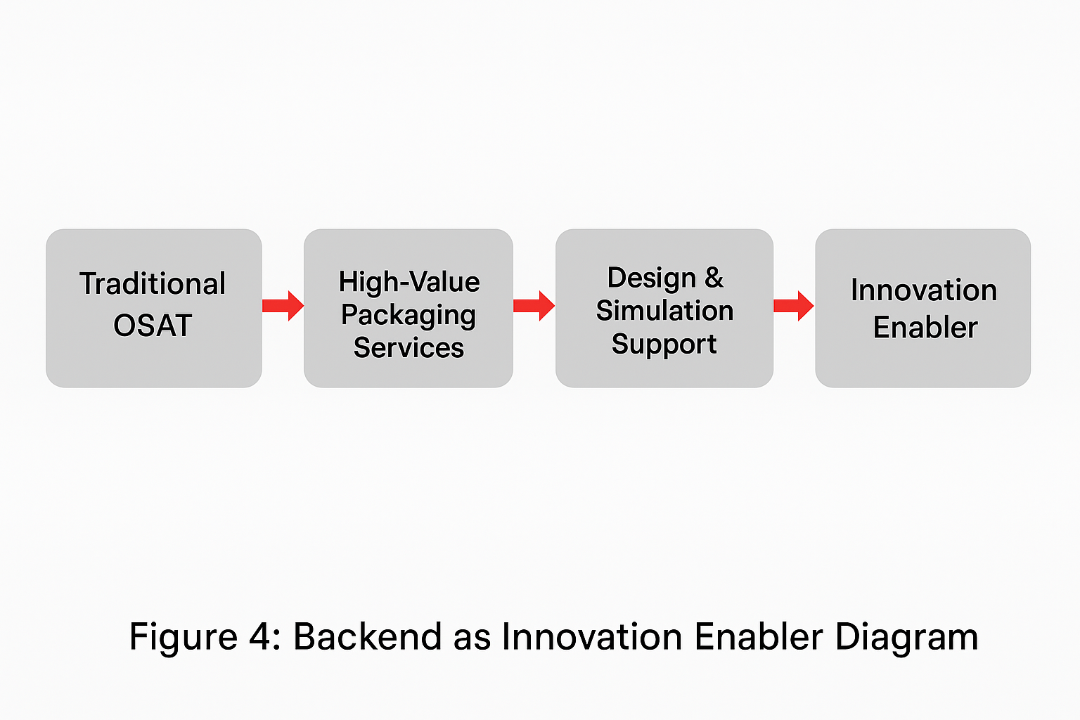
This figure illustrates the four-stage transformation of OSATs from traditional vendors to innovation enablers:
Stage | Name | Description |
|---|---|---|
1️⃣ | Traditional OSAT | Standard packaging and test services, focused on low cost and high volume |
2️⃣ | High-Value Packaging Services | FOWLP, SiP, 2.5D/3D offerings with partial design collaboration |
3️⃣ | Design & Simulation Support | Establishing co-design workflows and tools with IC/system teams |
4️⃣ | Innovation Enabler | Co-architecting heterogeneous systems with foundries, IDMs, fabless firms |
📈 Each stage moves rightward, representing value chain advancement and capability upgrading.
Real-world examples:
- ASE evolved from OSAT to FOCoS innovator collaborating with system companies
- Amkor is co-developing high-reliability packaging for automotive applications
- JCET built an SiP design center to offer integrated design services to fabless clients
Appendix: Key Terminology
Abbreviation | Full Term | Description |
|---|---|---|
OSAT | Outsourced Semiconductor Assembly and Test | 3rd-party packaging & testing vendors |
FOWLP | Fan-Out Wafer-Level Packaging | Advanced packaging with rerouted I/O pads |
TSV | Through-Silicon Via | Vertical interconnect for 3D IC stacking |
RDL | Redistribution Layer | Reroutes die I/Os for external connection |
CoWoS | Chip-on-Wafer-on-Substrate | TSMC's 2.5D packaging solution |
SiP | System-in-Package | Integration of multiple chips in one module |
FOCoS | Fan-Out Chip-on-Substrate | ASE's proprietary fan-out packaging solution |